
FlexCase & FlexBench
Datasheet – Pinout, Details, Drawing

FlexCase R (OEM)

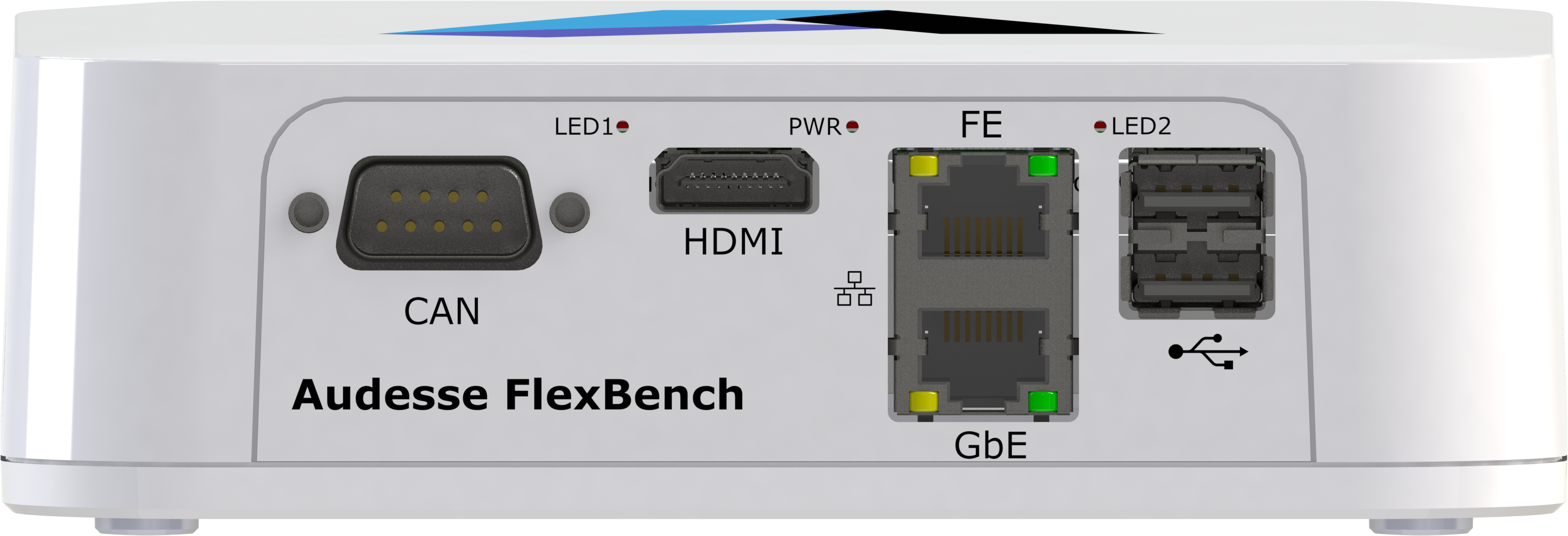
FlexBench

FlexCase E 1.0

FlexCase S

FlexCase E 2.0

FlexCase G
General Hardware Architecture

*Not all shown features available on every model.
Please see the hardware comparison guide or specific product pinouts for exact model information.*
Field Readiness
Deployable with production grade code using supported development environments.
Electromagnetic Compatibility
EMC has been completed for certain automotive applications, but is specific to each use case. Reach out for more details if EMC is required for your application.
- Radiated and conducted emissions
- Immunity to conducted transients on power leads
- Immunity to electrostatic discharge
- Immunity to electromagnetic fields
- Immunity to radiated electromagnetic fields
MATLAB Add-on Requirements
To program in MATLAB using the complimentary toolbox you will require the following add-ons from MATLAB:
- MATLAB
- Simulink
- MATLAB Coder
- Simulink Coder
- Embedded Coder
- (Optional) Stateflow
- (Optional) IEC Certification Kit for ISO 26262
| FlexCase S |
FlexBench |
|---|---|
|
C1 – 18 Pin header, C2 – 30 Pin header, Internal pin Current Version: 1.3 – Previous Versions |
Breakout Board (C3), Current Version: 1.2 – Previous Versions |


: FlexCase S Pro & FlexBench Only
: FlexBench Only
| Connector Pin # | Function | Application Comment |
|---|---|---|
| Power | ||
| FCS C2-H1 FB C2-7/8 FB C3-37/38/77/78 |
+ Supply Voltage | 8-36V (Unswitched)ⓘ Measure Supply Voltage ⓘ Measure Current |
| FCS C2-H3 FB C2-14 FB C3-74 |
Ignition Input |
On/Off Switch (Barrel jack automatically sets On) ⓘ Keep On |
| FCS C2-H2/G1 FB C2-1/2/3/4 FB C3-39/40/79/80 |
Ground | Grounds are common. Also avilable through barrel jack on FB. |
| FCS C2-D1 FB C2-9/10/11/12 FB C3-35/36/75/76 |
+5 Volt Supply |
For powering 5V components (2A Max) |
| +5V Supply Enable | Set to enable +5V EXT | |
| Sensors | ||
| IMU | Configurable,MISO, MOSI, CLK, CS,Int1, Int2 | |
| Buzzer | PWM Output (3000-5000 Hz) | |
| Board Version | Analog Measurement | |
| Power Good | Digital Measurement | |
| Ignition | Digital Measurement | |
| Coms | ||
| MCU-MPU SPI |
MCU (Typically Slave): MISO, MOSI, CLK, CS MPU (Typically Master): MISO, MOSI, CLK, CS |
|
| MPU-MPU GPIO Request | MCU <-> MPU | |
| MPU-MPU GPIO | MCU <-> MPU | |
| MPU Reset | ⚠ Set high for >200ms then release | |
| MPU Sleep | ⚠ User for low power applications | |
| LED 1 | MPU Activity Light | |
| LED 2 | User Controllable Light | |
| MPU-IoT Coms | ||
| UART | USB recommended DTR, MPU RX, MPU TX, CTS, RTS | |
| USB | USB | |
| VUSB Enable | Set to enable USB communication | |
| Reset | Digital Output. Set to enable. | |
| ON/OFF Enable | Digital Output. Set to enable. | |
| Ref Voltage Power | Digital Output. Set to enable. | |
| Status | Digital Measurement | |
| CAN | ||
| FCS C1-A1 FB C1-7 FB C3-27 |
MCU CAN0 High | FD capable. Also pin 7 DB9 on FB. |
| FCS C1-B1 FB C1-5 FB C3-28 |
MCU CAN0 Low | FD capable. Also pin 2 DB9 on FB. |
| MCU CAN0 Enable | Set to enable CANbus Enables all CAN channels on FlexCase S. | |
| FCS C1-C2 FB C1-3 FB C3-29 |
MCU CAN1 High | |
| FCS C1-C3 FB C1-1 FB C3-30 |
MCU CAN1 Low | |
| MCU CAN1 Enable | Set to enable CANbus. Connected to CAN0 Enable on FlesCase S. Enable bus termination via dip switch (FB Only) | |
| FCS C2-E2 FB C1-4 FB C3-69 |
MCU CAN2 High | |
| FCS C2-E3 FB C1-2 FB C3-70 |
MCU CAN2 Low | |
| MCU CAN2 Enable | Set to enable CANbus. Connected to CAN0 Enable on FlesCase S. Enable bus termination via dip switch (FB Only) | |
| Ethernet | ||
| FCS C1-A2 FB FE RJ45 |
MPU RX- | T568B Green, RJ45 pin 6. |
| FCS C1-A3 FB FE RJ45 |
MPU RX+ | T568B Green White, RJ45 pin 3. |
| FCS C1-B2 FB FE RJ45 |
MPU TX- | T568B Orange, RJ45 pin 2. |
| FCS C1-B3 FB FE RJ45 |
MPU TX+ | T568B Orange White, RJ45 pin 1. |
| FB GbE RJ45 | Gigabit Ethernet | GbE RJ45 Connector |
| USB | ||
| FCS C2-G2 FB USB |
USB 1 Data Positive | USB 2.0 Data Positive |
| FCS C2-G3 FB USB |
USB 1 Data Negative | USB 2.0 Data Negative |
| HDMI | ||
| FB HDMI | HDMI2.0 | HDMI 2.0 Available on via Mini HDMI connector |
| Standard Serial | ||
| FB C2-15 FB C3-33 |
RS232 TX / RS485 B | Optional on FlexBench 1.2 |
| FB C2-13 FB C3-34 |
RS232 RX / RS485 A | Optional on FlexBench 1.2 |
| Digital Outputs (DO) | ||
| Digital Output Enable | Enable all Digital Output banks | |
| FCS C2-A3 FB C1-38/40 FB C3-41/42 |
⚠ High Side Supply | FlexCase 1.3 Supplies all DO FlexBench 1.2 Supplies DO 1 – 5 |
| FB C1-37/39 FB C3-1/2 |
⚠ High Side Supply | FlexBench 1.2 Supplies DO 11 – 16 |
| FB C1-18/20 FB C3-61/62 |
⚠ High Side Supply | FlexBench 1.2 Supplies DO 6 – 10 |
| FCS C1-C1 FB C1-36 FB C3-43 |
MCU Digital Output 1 | High Side (DO/PWM) – Active HIGH on Revision 1.3. Active LOW on Revision 1.2 and below. Low Side (DO/PWM) – Active HIGH. |
| FCS C1-D3 FB C1-34 FB C3-44 |
MCU Digital Output 2 | High Side (DO/PWM) – Active HIGH on Revision 1.3. Active LOW on Revision 1.2 and below. Low Side (DO/PWM) – Active HIGH. |
| FCS C1-D2 FB C1-32 FB C3-45 |
MCU Digital Output 3 | High Side (DO/PWM) – Active HIGH on Revision 1.3. Active LOW on Revision 1.2 and below. Low Side (DO/PWM) – Active HIGH. |
| FCS C1-D1 FB C1-30 FB C3-46 |
MCU Digital Output 4 | High Side (DO/PWM) – Active HIGH on Revision 1.3. Active LOW on Revision 1.2 and below. Low Side (DO/PWM) – Active HIGH. |
| FCS C1-E3 FB C1-28 FB C3-47 |
MCU Digital Output 5 |
High Side (DO/PWM) – Active HIGH on Revision 1.3. Active LOW on Revision 1.2 and below. Low Side (DO/PWM) – Active HIGH. |
| FCS C1-E2 FB C1-16 FB C3-63 |
MCU Digital Output 6 | High Side (DO/PWM) – Active HIGH on Revision 1.3. Active LOW on Revision 1.2 and below. Low Side (DO/PWM) – Active HIGH. |
| FCS C1-E1 FB C1-14 FB C3-64 |
MCU Digital Output 7 | High Side (DO/PWM) – Active HIGH on Revision 1.3. Active LOW on Revision 1.2 and below. Low Side (DO/PWM) – Active HIGH. |
| FCS C1-F3 FB C1-12 FB C3-65 |
MCU Digital Output 8 | High Side (DO/PWM) – Active HIGH on Revision 1.3. Active LOW on Revision 1.2 and below. Low Side (DO/PWM) – Active HIGH. |
| FCS C1-F2 FB C1-10 FB C3-66 |
MCU Digital Output 9 | High Side (DO/PWM) – Active HIGH on Revision 1.3. Active LOW on Revision 1.2 and below. Low Side (DO/PWM) – Active HIGH. |
| FCS C1-F1 FB C1-8 FB C3-67 |
MCU Digital Output 10 | High Side (DO/PWM) – Active HIGH on Revision 1.3. Active LOW on Revision 1.2 and below. Low Side (DO/PWM) – Active HIGH. |
| FCS C2-A2 FB C1-35 FB C3-3 |
MCU Digital Output 11 | High Side (DO/PWM) – Active HIGH on Revision 1.3. Active LOW on Revision 1.2 and below. Low Side (DO/PWM) – Active HIGH. |
| FCS C2-B3 FB C1-33 FB C3-4 |
MCU Digital Output 12 | High Side (DO/PWM) – Active HIGH on Revision 1.3. Active LOW on Revision 1.2 and below. Low Side (DO/PWM) – Active HIGH. |
| FCS C2-B2 FB C1-31 FB C3-5 |
MCU Digital Output 13 | High Side (DO/PWM) – Active HIGH on Revision 1.3. Active LOW on Revision 1.2 and below. Low Side (DO/PWM) – Active HIGH. |
| FCS C2-B1 FB C1-29 FB C3-6 |
MCU Digital Output 14 | High Side (DO/PWM) – Active HIGH on Revision 1.3. Active LOW on Revision 1.2 and below. Low Side (DO/PWM) – Active HIGH. |
| FCS C2-C3 FB C1-27 FB C3-7 |
MCU Digital Output 15 | High Side (DO/PWM) – Active HIGH on Revision 1.3. Active LOW on Revision 1.2 and below. Low Side (DO/PWM) – Active HIGH. |
| FCS C2-C1 FB C1-25 FB C3-8 |
MCU Digital Output 16 | High Side (DO/PWM) – Active HIGH on Revision 1.3. Active LOW on Revision 1.2 and below. Low Side (DO/PWM) – Active HIGH. |
| Digital Inputs (DI) | ||
| MCU Digital Input Pull Up Enable | Set high to enable Digital Input Pull Ups | |
| FCS C2-C2 FB C1-19 FB C3-21 |
MCU Digital Input 1 | DI/QUAD2 B/PWM |
| FCS C2-D2 FB C1-17 FB C3-22 |
MCU Digital Input 2 | DI/QUAD2 I/PWM |
| FCS C2-D3 FB C1-15 FB C3-23 |
MCU Digital Input 3 | DI/QUAD2 A/PWM |
| FCS C2-F1 FB C1-13 FB C3-24 |
MCU Digital Input 4 | DI/QUAD1 B/PWM |
| FCS C2-F2 FB C1-11 FB C3-25 |
MCU Digital Input 5 | DI/QUAD1 I/PWMAlternative PWM on FCS1.3 |
| FCS C2-F3 FB C1-9 FB C3-26 |
MCU Digital Input 6 | DI/QUAD1 A/PWM |
| FCS C2-E1 | MCU Digital Input 7 | DI/PWM |
| FCS C2-A1 | MCU Digital Input 8 | DI/PWM |
| FB C2-24 FB C3-59 |
MPU Digital Input 1 | DI |
| FB C2-22 FB C3-60 |
MPU Digital Input 2 | DI |
| FB C2-23 FB C3-19 |
MPU Digital Input 3 | DI |
| FB C2-21 FB C3-20 |
MPU Digital Input 4 | DI |
| FB C2-20 FB C3-71 |
MPU Digital Input 5 | DI |
| FB C2-18 FB C3-72 |
MPU Digital Input 6 | DI |
| FB C2-19 FB C3-31 |
MPU Digital Input 7 | DI |
| FB C2-17 FB C3-32 |
MPU Digital Input 8 | DI |
| Analog Input (AIn) | ||
| FCS C2-J1 FB C2-29 FB C3-16 |
MCU Analog Input 6 | 0-36V (configurable) |
| FCS C2-J2 FB C2-31 FB C3-15 |
MCU Analog Input 5 | 0-36V (configurable) |
| FCS C2-J3 FB C2-33 FB C3-14 |
MCU Analog Input 4 | 0-36V (configurable) |
| FCS C2-K1 FB C2-35 FB C3-13 |
MCU Analog Input 3 | 0-36V (configurable) |
| FCS C2-K2 FB C2-37 FB C3-12 |
MCU Analog Input 2 | 0-36V (configurable) |
| FCS C2-K3 FB C2-39 FB C3-11 |
MCU Analog Input 1 | 0-36V (configurable) |
| FB C2-40 FB C3-51 |
MPU Analog Input 1 | 0-36V (configurable) |
| FB C2-38 FB C3-52 |
MPU Analog Input 2 | 0-36V (configurable) |
| FB C2-36 FB C3-53 |
MPU Analog Input 3 | 0-36V (configurable) |
| FB C2-34 FB C3-54 |
MPU Analog Input 4 | 0-36V (configurable) |
| FB C2-32 FB C3-55 |
MPU Analog Input 5 | 0-36V (configurable) |
| FB C2-30 FB C3-56 |
MPU Analog Input 6 | 0-36V (configurable) |
| FB C2-28 FB C3-57 |
MPU Analog Input 7 | 0-36V (configurable) |
| FB C2-26 FB C3-58 |
MPU Analog Input 8 | 0-36V (configurable) |
| FlexCase E 2.0 |
FlexCase G |
|---|---|
|
J1 – 64 Pin header, Internal pin |
J1 – 60 Pin Header, J2 – 94 Pin Header, Internal pin. |


: FlexCase Pro Only
| Connector Pin # | Function | Application Comment |
|---|---|---|
| Power | ||
| FCE J1-Q1/Q2 FCG J2-3/4 |
+ Supply Voltage | 8-36V (Unswitched)ⓘ Measure Supply Voltage |
| FCE J1-O2 FCG J2-8 |
Ignition Input |
5-36V On/Off Switch. Wake on CAN/LIN available. ⓘ Keep On |
| FCE J1-Q3/Q4 FCG J2-5/6 |
Ground | Grounds are common. |
| FCE J1-P4 FCG J2-77 |
Vcc Supply |
For powering 12/24V nominal components (200mA Max) |
| FCE J1-P3 FCG J2-90/91/92/93/94 |
+5 Volt Supply |
For powering 5V components (200mA Max). Requires enabling +5V supply. |
| FCE J1-P2 FCGJ2-68/69/70/71/72 |
Sensor Ground | For powering external components (200mA Max). |
| +5V Supply Enable | Set to enable +5V EXT | |
| Sensors | ||
| IMU | Configurable,MISO, MOSI, CLK, CS,Int1, Int2 | |
| Board Version | Analog Measurement | |
| Power Good | Digital Measurement | |
| Ignition | Digital Measurement | |
| Coms | ||
| MCU-MPU SPI | MCU (Typically Slave): MISO, MOSI, CLK, CS
MPU (Typically Master): MISO, MOSI, CLK, CS |
|
| MCU-MPU UART | MCU : RX, TX
MPU : RX, TX |
|
| MPU-MPU GPIO Request | MCU <-> MPU | |
| MPU-MPU GPIO | MCU <-> MPU | |
| MPU Reset | ⚠ Set high for >200ms then release | |
| MPU Sleep | ⚠ User for low power applications | |
| MPU-IoT Coms | ||
| UART | USB recommended DTR, MPU RX, MPU TX, CTS, RTS | |
| USB | USB | |
| VUSB Enable | Set to enable USB communication | |
| Reset | Digital Output. Set to enable. | |
| ON/OFF Enable | Digital Output. Set to enable. | |
| Ref Voltage Power | Digital Output. Set to enable. | |
| Status | Digital Measurement | |
| CAN | ||
| MCU CAN Enable | Set to enable all CANbus | |
| FCE J1-A4 FCG J1-12 |
MCU CAN0 High | FD capable. |
| FCE J1-A3 FCG J1-13 |
MCU CAN0 Low | FD capable. |
| FCE J1-B4 FCG J1-27 |
MCU CAN1 High | FD capable. |
| FCE J1-B3 FCG J1-28 |
MCU CAN1 Low | FD capable. |
| FCE J1-C4 FCG J1-42 |
MCU CAN2 High | FD capable. |
| FCE J1-C3 FCG J1-43 |
MCU CAN2 Low | FD capable. |
| FCE J1-D4 FCG J1-38 |
MCU CAN3 High | FD capable. |
| FCE J1-D3 FCG J1-39 |
MCU CAN3 Low | FD capable. |
| FCE J1-E4 FCG J1-36 |
MCU CAN4 High | FD capable. Wake-on-CAN. |
| FCE J1-E3 FCG J1-37 |
MCU CAN4 Low | FD capable. Wake-on-CAN. |
| FCE J1-E2 FCG J1-21 |
MCU CAN5 V+ | Isolated CANbus. Supply 4.5-5.5V W.R.T. V-. To use as a standard bus connect to +5V supply. |
| FCE J1-D2 FCG J1-6 |
MCU CAN5 High | Isolated CANbus. |
| FCE J1-D1 FCG J1-7 |
MCU CAN5 Low | Isolated CANbus. |
| FCE J1-E1 FCG J1-22 |
MCU CAN5 V- | Isolated CANbus ground. To use as standard bus connect to GND. |
| LIN | ||
| FCE J1-O1 FCG J2-9 |
LIN 1 | RX, TX,ENABLE,Commander/Responder SW Select |
| FCG J2-30 | LIN 2 |
RX, TX,ENABLE,Commander/Responder SW Select |
| PLC | ||
| SPI Communication to QCA | MCU (Typically Master): MISO, MOSI, CLK, CS | |
| Mux. | Control Pilot & Proximity Pilot | CP, PP |
| Ethernet | ||
| FCE J1-J1 FCG J1-56 |
MCU ETH+ | |
| FCE J1-J2 FCG J1-41 |
MCU ETH- | |
| FCE J1-D2* FCG J2-47 |
MPU MX1+ | T568B Orange White, RJ45 pin 1. (Fast Eth. TX+) *Available for volume order. |
| FCE J1-D1* FCG J2-25 |
MPU MX1- | T568B Orange, RJ45 pin 2. (Fast Eth. TX-) *Available for volume order. |
| FCE J1-E2* FCG J2-48 |
MPU MX2+ | T568B Green White, RJ45 pin 3. (Fast Eth. RX+) *Available for volume order. |
| FCG J2-27 | MPU MX3+ | T568B Blue, RJ45 pin 4 |
| FCG J2-49 | MPU MX3- | T568B Blue White, RJ45 pin 5 |
| FCE J1-E1* FCG J2-26 |
MPU MX2- | T568B Green, RJ45 pin 6. (Fast Eth. RX-) *Available for volume order. |
| FCG J2-28 | MPU MX4+ | T568B Brown White, RJ45 pin 7 |
| FCG J2-50 | MPU MX4- | T568B Brown, RJ45 pin 8 |
| USB | ||
| FCE J1-J3* FCG J2-39 |
USB OTG | Apply HIGH signal to set slave mode. *Available for volume order. |
| FCE J1-K1* FCG J2-16 |
USB 1 Data Positive | USB 2.0 Data Positive (green). *Available for volume order. |
| FCE J1-K2* FCG J2-38 |
USB 1 Data Negative | USB 2.0 Data Negative (white). *Available for volume order. |
| Standard Serial | ||
| FCG J2-46 | RS232 TX | MPU Based UART |
| FCG J2-24 | RS232 RX | MPU Based UART |
| Digital Outputs (DO) | ||
| Lowside Digital Output Enable | Set to enable all Lowside Digital Output banks | |
| High Side Digital Output Feedback | Set to choose which high side outputs to read feadback pin | |
| Low Side Digital Output Feedback | Feedback reading logic | |
| Bank 1 | ||
| FCE J1-P1 FCG J2-1 |
High Side Supply | External Pin Supplies DO 1 – 10 |
| FCE J1-A1 FCG J1-5 |
High Side Digital Output 1 | Set DO/PWM, Read Feedback/Fault, Note: Half Bridge Capable |
| FCE J1-A1 FCG J1-46 |
Low Side Digital Output 1 | Set DO/PWM, Read Feedback/Fault, Note: Half Bridge Capable |
| FCE J1-A2 FCG J1-20 |
High Side Digital Output 2 | Set DO/PWM, Read Feedback/Fault, Note: Half Bridge Capable |
| FCE J1-A2 FCG J1-31 |
Low Side Digital Output 2 | Set DO/PWM, Read Feedback/Fault, Note: Half Bridge Capable |
| FCE J1-B1 FCG J1-52 |
High Side Digital Output 3 | Set DO/PWM, Read Feedback/Fault, Note: Half Bridge Capable |
| FCE J1-B1 FCG J1-16 |
Low Side Digital Output 3 | Set DO/PWM, Read Feedback/Fault, Note: Half Bridge Capable |
| FCE J1-B2 FCG J1-51 |
High Side Digital Output 4 | Set DO/PWM, Read Feedback/Fault, Note: Half Bridge Capable |
| FCE J1-B2 FCG J1-1 |
Low Side Digital Output 4 | Set DO/PWM, Read Feedback/Fault, Note: Half Bridge Capable |
| FCE J1-C1 FCG J1-54 |
High Side Digital Output 5 | Set DO/PWM, Read Feedback/Fault, Note: Half Bridge Capable |
| FCE J1-C1 FCG J1-47 |
Low Side Digital Output 5 | Set DO/PWM, Read Feedback/Fault, Note: Half Bridge Capable |
| FCE J1-C2 FCG J1-53 |
High Side Digital Output 6 | Set DO/PWM, Read Feedback/Fault, Note: Half Bridge Capable |
| FCE J1-C2 FCG J1-32 |
Low Side Digital Output 6 | Set DO/PWM, Read Feedback/Fault, Note: Half Bridge Capable |
| FCE J1-G1 FCG J1-44 |
High Side Digital Output 7 | Set DO/PWM, Read Feedback/Fault, Note: Half Bridge Capable |
| FCE J1-G1 FCG J1-17 |
Low Side Digital Output 7 | Set DO/PWM, Read Feedback/Fault, Note: Half Bridge Capable |
| FCE J1-G2 FCG J1-59 |
High Side Digital Output 8 | Set DO/PWM, Read Feedback/Fault, Note: Half Bridge Capable |
| FCE J1-G2 FCG J1-2 |
Low Side Digital Output 8 | Set DO/PWM, Read Feedback/Fault, Note: Half Bridge Capable |
| FCE J1-H1 FCG J1-45 |
High Side Digital Output 9 | Set DO/PWM, Read Feedback/Fault, Note: Half Bridge Capable |
| FCE J1-H1 FCG J1-48 |
Low Side Digital Output 9 | Set DO/PWM, Read Feedback/Fault, Note: Half Bridge Capable |
| FCE J1-H2 FCG J1-60 |
High Side Digital Output 10 | Set DO/PWM, Read Feedback/Fault, Note: Half Bridge Capable |
| FCE J1-H2 FCG J1-33 |
Low Side Digital Output 10 | Set DO/PWM, Read Feedback/Fault, Note: Half Bridge Capable |
| Bank 2 | ||
| High Side Supply | Internal VBatt Supplies DO 11 – 18 & 3 Phase | |
| FCE J1-L1 FCG J1-14 |
High Side Digital Output 11 | Set DO/PWM, Read Feedback/Fault, Note: Half Bridge Capable |
| FCE J1-L1 FCG J1-18 |
Low Side Digital Output 11 | Set DO/PWM, Read Feedback/Fault, Note: Half Bridge Capable |
| FCE J1-L2 FCG J1-29 |
High Side Digital Output 12 | Set DO/PWM, Read Feedback/Fault, Note: Half Bridge Capable |
| FCE J1-L2 FCG J1-3 |
Low Side Digital Output 12 | Set DO/PWM, Read Feedback/Fault, Note: Half Bridge Capable |
| FCE J1-M1 FCG J1-15 |
High Side Digital Output 13 | Set DO/PWM, Read Feedback/Fault, Note: Half Bridge Capable |
| FCE J1-M1 FCG J1-49 |
Low Side Digital Output 13 | Set DO/PWM, Read Feedback/Fault, Note: Half Bridge Capable |
| FCE J1-M2 FCG J1-30 |
High Side Digital Output 14 | Set DO/PWM, Read Feedback/Fault, Note: Half Bridge Capable |
| FCE J1-M2 FCG J1-34 |
Low Side Digital Output 14 | Set DO/PWM, Read Feedback/Fault, Note: Half Bridge Capable |
| FCE J1-N1 FCG J2-74 |
High Side Digital Output 15 | Set DO/PWM, Read Feedback/Fault, Note: Half Bridge Capable |
| FCE J1-N1 FCG J1-19 |
Low Side Digital Output 15 | Set DO/PWM, Read Feedback/Fault, Note: Half Bridge Capable |
| FCE J1-N2 FCG J2-73 |
High Side Digital Output 16 | Set DO/PWM, Read Feedback/Fault, Note: Half Bridge Capable |
| FCE J1-N2 FCG J1-4 |
Low Side Digital Output 16 | Set DO/PWM, Read Feedback/Fault, Note: Half Bridge Capable |
| FCG J1-50 | Low Side Digital Output 17 | Set DO/PWM, Read Feedback/Fault, Note: Half Bridge Capable |
| FCG J1-35 | Low Side Digital Output 18 | Set DO/PWM, Read Feedback/Fault, Note: Half Bridge Capable |
| Digital Output 3 Phase | Set to enable high current 3-phase output, Driver SPI diagnostics. | |
| FCG J2-51 | Digital Output – Phase A | High Side (DO/PWM) Low Side (DO/PWM) |
| FCG J2-29 | Digital Output – Phase B | High Side (DO/PWM) Low Side (DO/PWM) |
| FCG J2-7 | Digital Output – Phase C | High Side (DO/PWM) Low Side (DO/PWM) |
| Digital Inputs (DI) | ||
| Digital Input Pull Up Enable 1 | Set high to enable Digital Input 1-6 Pull Ups | |
| FCE J1-K1 FCG J2-18 |
Digital Input 1 | DI/PWM |
| FCE J1-K2 FCG J2-40 |
Digital Input 2 | DI/PWM |
| FCE J1-J3 FCG J2-19 |
Digital Input 3 | DI/PWM |
| FCE J1-J4 FCG J2-41 |
Digital Input 4 | DI/PWM |
| FCE J1-K3 FCG J2-20 |
Digital Input 5 | DI/PWM |
| FCE J1-K4 FCG J2-42 |
Digital Input 6 | DI/PWM |
| Digital Input Pull Up Enable 2 | Set high to enable Digital Input 7-12 Pull Ups | |
| FCE J1-L3 FCG J2-21 |
Digital Input 7 | DI/PWM |
| FCE J1-L4 FCG J2-43 |
Digital Input 8 | DI/PWM |
| FCE J1-M3 FCG J2-22 |
Digital Input 9 | DI/PWM |
| FCE J1-M4 FCG J2-44 |
Digital Input 10 | DI/PWM |
| FCE J1-N3 FCG J2-23 |
Digital Input 11 | DI/PWM |
| FCE J1-N4 FCG J2-45 |
Digital Input 12 | Control Pilot | DI/PWM. Control Pilot charge status ready. Max voltage is 13V if PLC is used. |
| Analog Input (AIn) | ||
| FCE J1-F3 FCG J1-8 |
Analog Input 1 | 0-36V (configurable) |
| FCE J1-F4 FCG J1-23 |
Analog Input 2 | 0-36V (configurable) |
| FCE J1-G3 FCG J1-9 |
Analog Input 3 | 0-36V (configurable) |
| FCE J1-G4 FCG J1-24 |
Analog Input 4 | 0-36V (configurable) |
| FCG J2-80 | Analog Input 5 | 0-36V (configurable) |
| FCG J2-58 | Analog Input 6 | 0-36V (configurable) |
| FCG J2-81 | Analog Input 7 | 0-36V (configurable) |
| FCG J2-59 | Analog Input 8 | 0-36V (configurable) |
| FCE J1-H3 FCG J1-10 |
Analog Input 9 | 0-36V (configurable) |
| FCE J1-H4 FCG J1-25 |
Analog Input 10 | 0-36V (configurable) |
| FCE J1-F1 FCG J1-11 |
Analog Input 11 | 0-36V (configurable) |
| FCE J1-F2 FCG J1-26 |
Analog Input 12 | Proximity Pilot | 0-36V (configurable) |
| FCE J1-O3 FCG J1-55 |
Analog Input 29 | Analog Output 1 | 0-36V (configurable), DAC is via MCP4922 on SPI ENABLE, SOUT, SIN, SCK, CS |
| FCE J1-O4 FCG J1-40 |
Analog Input 30 | Analog Output 2 | 0-36V (configurable), DAC is via MCP4922 on SPI ENABLE, SOUT, SIN, SCK, CS |
| FCG J2-82 | Analog Input 13 | 0-36V (configurable) |
| FCG J2-60 | Analog Input 14 | 0-36V (configurable) |
| FCG J2-83 | Analog Input 15 | 0-36V (configurable) |
| FCG J2-61 | Analog Input 16 | 0-36V (configurable) |
| FCG J2-84 | Analog Input 17 | 0-36V (configurable) |
| FCG J2-62 | Analog Input 18 | 0-36V (configurable) |
| FCG J2-85 | Analog Input 19 | 0-36V (configurable) |
| FCG J2-63 | Analog Input 20 | 0-36V (configurable) |
| FCG J2-86 | Analog Input 21 | 0-36V (configurable) |
| FCG J2-64 | Analog Input 22 | 0-36V (configurable) |
| FCG J2-87 | Analog Input 23 | 0-36V (configurable) |
| FCG J2-65 | Analog Input 24 | 0-36V (configurable) |
| FCG J2-88 | Analog Input 25 | 0-36V (configurable) |
| FCG J2-66 | Analog Input 26 | 0-36V (configurable) |
| FCG J2-89 | Analog Input 27 | 0-36V (configurable) |
| FCG J2-67 | Analog Input 28 | 0-36V (configurable) |
| Expansion Connector |
Turnkey support available for volume orders. | |
| LSHM | Power Reserved | 3.3 V, 5.0V , VBATT, GND |
| FCG J1-57/58 FCG J2-10/11/12/31/32/3352/53/54/55/56/57/75/76/78/79 |
Header Pins Reserved | 50V rating. 500mA-1A capacity on pins. Contact Audesse for design files. |
| LSHM | GPIO Reserved | Request, Sleep, Reset |
| LSHM | USB Reserved | USB 2.0 D+, USB 2.0 D+ |
| LSHM | CAN Reserved | CAN 3 High, CAN 3 Low |
| LSHM | UART Reserved | RX, TX |
| LSHM | I2C Reserved | SCL, SDA |
| LSHM | SPI Reserved | SIN, SOUT, CLK, CS0, CS1 |
| FlexCase E | FlexCase R (OEM) |
|---|---|

Color legend: C1 – 18 Pin header, C2 – 30 Pin header, Internal pin. = MPU Version only (CM4) Current Version: 1.0 |
 
Color legend: C1 – 8 Pin header, C2 – 30 Pin header, C3 – 4 Pin header, C4 – 30 Pin header, Internal pin. = MPU Version only (CM4) Current Version: 1.0 |

Note: The FlexCase E and R (OEM SBC) are almost identical except for a change of connectors. The FlexCase E is intented for IP rated applications whereas the OEM version is more suited for custom integrations.
| FlexCase E Pin # |
OEM SBC Pin # |
Function | Application Comment |
|---|---|---|---|
| Power | |||
| C2-H1 | C1-1 | + Supply Voltage | 8-36V (Unswitched)ⓘ Measure Supply Voltage ⓘ Measure Current |
| C2-H3 | C1-6 | Ignition Input |
On/Off Switch ⓘ Keep On |
| C2-H2 | C1-2 | Ground | Grounds are common |
| C2-G1 | C2-23 C4-29 |
Ground | Grounds are common |
| C2-D1 | C1-5 C2-21 |
+5 Volt Supply |
For powering 5V components. 2A Max |
| +5V Supply Enable | Set to enable +5V EXT | ||
| Sensors | |||
| IMU | ConfigurableMISO, MOSI, CLK, CS,Int1, Int2 | ||
| Board Version | Analog Measurement | ||
| Power Good | Digital Measurement | ||
| Ignition | Digital Measurement | ||
| Coms | |||
| MCU-MPU SPI | MCU (Typically Slave): MISO, MOSI, CLK, CS
MPU (Typically Master): MISO, MOSI, CLK, CS1 |
||
| MCU-MPU UART | MCU <-> MPU | ||
| MPU-MPU GPIO 1 | MCU <-> MPU | ||
| MPU-MPU GPIO 0 | MCU <-> MPU | ||
| MPU Reset | ⚠ Set high for >200ms then release | ||
| MPU Sleep | ⚠ User for low power applications | ||
| MPU-IoT Coms | Nimbelink/Airgain Skywire Compatible | ||
| UART | USB recommended DTR, MPU RX, MPU TX, CTS, RTS | ||
| USB | USB | ||
| VUSB Enable | Set to enable USB communication | ||
| Reset | Digital Output. Set to enable. | ||
| ON/OFF Enable | Digital Output. Set to enable. | ||
| Ref Voltage Power | Digital Output. Set to enable. | ||
| Status | Digital Measurement | ||
| CAN | |||
| C1-A1 | C4-23 C1-3 |
MCU CAN0 High | FD capable |
| C1-B1 | C4-21 C1-7 |
MCU CAN0 Low | FD capable |
| MCU CAN0 Enable | Set to enable CANbus | ||
| C1-C2 | C4-19 C1-4 |
MCU CAN1 High | FD capable |
| C1-C3 | C4-17 C1-8 |
MCU CAN1 Low | FD capable |
| MCU CAN1 Enable | Set to enable CANbus | ||
| C1-A2 | C2-22 | MCU CAN2 High | FD capable |
| C1-B2 | C2-24 | MCU CAN2 Low | FD capable |
| MCU CAN2 Enable | Set to enable CANbus | ||
| C1-A3 | C2-18 | MCU CAN3 High | FD capable |
| C1-B3 | C2-20 | MCU CAN3 Low | FD capable |
| MCU CAN3 Enable | Set to enable CANbus | ||
| LIN | |||
| C2-C3 | C4-25 | MCU LIN Out | RX, TX,ENABLE |
| Ethernet | |||
| C1-D1 | C2-1 | MPU MX1 Positive | T568B Orange White, RJ45 pin 1 |
| C1-D2 | C2-8 | MPU MX1 Negative | T568B Orange, RJ45 pin 2 |
| C1-D3 | C2-5 | MPU MX2 Positive | T568B Green White, RJ45 pin 3 |
| C1-E1 | C2-10 | MPU MX3 Positive | T568B Blue, RJ45 pin 4 |
| C1-E2 | C2-12 | MPU MX3 Negative | T568B Blue White, RJ45 pin 5 |
| C1-E3 | C2-7 | MPU MX2 Negative | T568B Green, RJ45 pin 6 |
| C1-F1 | C2-9 | MPU MX4 Positive | T568B Brown White, RJ45 pin 7 |
| C1-F2 | C2-11 | MPU MX4 Negative | T568B Brown, RJ45 pin 8 |
| USB | |||
| C2-A3 | C2-17 | USB 1 Data Positive | USB 2.0 Data Positive |
| C2-A2 | C2-19 | USB 1 Data Negative | USB 2.0 Data Negative |
| USB 2 | USB 2.0 Available on via USB C connector | ||
| HDMI | |||
| HDMI2.0 | HDMI 2.0 Available on via Mini HDMI connector | ||
| RS | |||
| C2-G3 | C2-16 | RS 232 TX | |
| C2-G2 | C2-14 | RS 232 RX | |
| C2-B3 | C2-13 | RS 485 A | |
| C2-B2 | C2-15 | RS 485 B | |
| Digital Outputs (DO) |
|||
| Bank 1 | |||
| Digital Output Enable | Set to enable Digital Outputs | ||
| C1-F3 | C2-29 | High Side Supply | Supplies DO 1 – 4 |
| C1-C1 | C2-26 | MCU Digital Output 1 | High Side (DO/PWM) Low Side (DO/PWM) |
| C2-A1 | C2-28 | MCU Digital Output 2 | High Side (DO/PWM) Low Side (DO/PWM) |
| C2-B1 | C2-30 | MCU Digital Output 3 | High Side (DO/PWM) Low Side (DO/PWM) |
| C2-C1 | C2-25 | MCU Digital Output 4 | High Side (DO/PWM) Low Side (DO/PWM) |
| Bank 2 | |||
| Digital Output Enable | Set to enable Digital Outputs | ||
| C4-2 | High Side Supply | Supplies DO 5 – 8 | |
| C4-6 | MCU Digital Output 5 | High Side (DO/PWM) Low Side (DO/PWM) |
|
| C4-1 | MCU Digital Output 6 | High Side (DO/PWM) Low Side (DO/PWM) |
|
| C4-3 | MCU Digital Output 7 | High Side (DO/PWM) Low Side (DO/PWM) |
|
| C4-4 | MCU Digital Output 8 | High Side (DO/PWM) Low Side (DO/PWM) |
|
| Digital Inputs (DI) |
|||
| Digital Input Enable | Set high to enable Digital Input Pull Ups | ||
| C2-F3 | C1-8 | MCU Digital Input 1 | DI /PWM |
| C2-F2 | C1-10 | MCU Digital Input 2 | DI /PWM |
| C2-F1 | C1-12 | MCU Digital Input 3 | DI /PWM |
| C2-E3 | C1-14 | MCU Digital Input 4 | DI /PWM |
| C2-E2 | C1-16 | MCU Digital Input 5 | DI /PWM |
| C2-E1 | C1-18 | MCU Digital Input 6 | DI /PWM |
| C2-D3 | C1-20 | MCU Digital Input 7 | DI /PWM |
| C2-D2 | C1-22 | MCU Digital Input 8 | DI /PWM |
| C2-C2 | C1-24 | MCU Digital Input 9 | DI /PWM |
| C1-26 | MCU Digital Input 10 | DI /PWM | |
| C1-28 | MCU Digital Input 11 | DI /PWM | |
| C1-30 | MCU Digital Input 12 | DI /PWM | |
| Analog Input (AIn) |
|||
| C2-K3 | C4-5 | MCU Analog Input 1 | 0-36V Configurable |
| C2-K2 | C4-7 | MCU Analog Input 2 | 0-36V Configurable |
| C2-K1 | C4-9 | MCU Analog Input 3 | 0-36V Configurable |
| C2-J3 | C4-11 | MCU Analog Input 4 | 0-36V Configurable |
| C2-J2 | C4-13 | MCU Analog Input 5 | 0-36V Configurable |
| C2-J1 | C4-15 | MCU Analog Input 6 | 0-36V Configurable |
| C3-3 | MCU Analog Diff 1 High | 500mV Difference. High voltage tolerant. | |
| C3-4 | MCU Analog Diff 1 Low | 500mV Difference. High voltage tolerant. | |
| C3-1 | MCU Analog Diff 2 High | 500mV Difference. High voltage tolerant. | |
| C3-2 | MCU Analog Diff 2 Low | 500mV Difference. High voltage tolerant. | |
| RESERVED Board to board |
Available for volume orders. | ||
| GPIO Reserved | GPIO1, GPIO2, GPIO3, GPIO4, GPIO5, GPIO6 | ||
| Analog Input Reserved | AIN0, AIN1, AIN2, AIN3, AIN4 | ||
| UART Reserved | RX, TX | ||
| I2C Reserved | SCL, SDA | ||
| SPI Reserved | SIN, SOUT, CLK, CS0, CS1 |
FlexCase S/E/G
Please leave at least 2” in front of the enclosure (connector location) for cable management.
- FlexCase S
- 4250000872 Pins for 20GXL, 18TXL wire & 5991111615 hand tool
- 4250000873 Pins for 18GXL, 16TXL, 16GXL wire & 5991111616 hand tool
- FlexCase E
- Please contact us for additional connectors and pins.
- FlexCase G
- Please contact us for additional connectors and pins.
OEM SBC

*All Dimensions in millimeters
Please leave at least 1” in front of connectors for cable management.
FlexBench
Header I/O pins on the back of the FlexBench are Samtec TFM-120-02-L-DH. If a custom board is desired we recommend:
- Download the design files for the breakout board.
- You can swap the Samtec SFM counterpart if desired. An example part number would be SFM-120-xx-x-x-D(H) where x is selectable based on your application. You can design horizontal or vertical boards.
- You may want to add bulk capacitors and overvoltage protection to your custom circuit if desired.
- Use the provided mount holes to secure your PCB.
- Check the positioning of your design using the provided CAD model.
- You can get the board manufactured and assembled at your favourite PCBA supplier.
Need more than what is on board? Our products are easily expandable with our CANbus and Ethernet modules. There is a wide range of available add-ons. Contact us to add any of the following:
| Type | Input | Output |
|---|---|---|
| Analog |
|
|
| Digital |
|
|
| Specialty |
|
|
How Does It Work?
The FlexCase is easily expanded by attaching almost any device to the CAN bus or Ethernet network present. We have a number of pre-approved add-ons listed above which make the task even easier and are automatically setup.

